
UNIVERSITY OF WEST ATTICA
SCHOOL OF ENGINEERING
DEPARTMENT OF COMPUTER ENGINEERING AND INFORMATICS
University of West Attica · Department of Computer Engineering and Informatics
Logic Design
Vasileios Evangelos Athanasiou
Student ID: 19390005
Supervision
Supervisor: Konstantinos Efstathiou, Professor
Supervisor: Ioannis Amorginos, Applications Lecturer
Co-supervisor: Eleni Tsalera, Academic Scholar
Co-supervisor: Anastasios Tsilikounas, Laboratory Teaching Staff
Athens, May 2021
This project explores the design, simulation, and theoretical analysis of various shift registers and sliders using the Multisim simulator. It was developed as part of a Digital Design workshop at the University of West Attica.
The core focus is on understanding information transfer and storage through logic circuits, specifically using D flip-flops and integrated circuits such as the 74LS194.
| Section | Folder/File | Description |
|---|---|---|
| 1 | assign/ |
Assignment material for the Registers and Sliders workshop |
| 1.1 | assign/ASSIGNMENT 4.pdf |
Assignment description in English |
| 1.2 | assign/ΕΡΓΑΣΙΑ 4.pdf |
Assignment description in Greek |
| 2 | docs/ |
Documentation covering registers and sliders theory |
| 2.1 | docs/Registers-Sliders.pdf |
English documentation for registers and sliders |
| 2.2 | docs/Καταχωρητές-Ολισθητές.pdf |
Greek documentation for registers and sliders |
| 3 | multisim/ |
Multisim register and slider simulation files |
| 3.1 | multisim/8-bit-Register.ms14 |
8-bit register simulation |
| 3.2 | multisim/generalSlider.ms14 |
General slider simulation |
| 4 | README.md |
Project documentation |
| 5 | INSTALL.md |
Usage instructions |
- Software: NI Multisim (for circuit design and simulation)
- Key Hardware (Simulated):
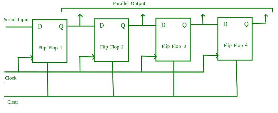
- 74LS194N: 4-bit bidirectional universal shift register
- Logic Gates: AND, OR, NOR, NAND, XOR, XNOR, NOT
- Input/Output: VCC sources (5V), Ground, lamps as indicators, interactive switches (Spacebar for CLOCK, 'C' for CLEAR)
- Measurement Tools: Oscilloscope for signal analysis
Analysis of the 74LS194 integrated circuit across multiple states:
- Initial State: Set via parallel inputs
- Clock Pulse Behavior: Step-by-step observation of data movement after each clock pulse
- Operational Modes:
- SIPO: Serial Input, Parallel Output
- PISO: Parallel Input, Serial Output
- Shift Directions: Both right and left shift operations implemented
This exercise demonstrates data transfer between two 4-bit registers to form an 8-bit storage system, illustrating how smaller register units can be cascaded to handle larger bit-widths in digital computing.
| Chapter | Title | Description |
|---|---|---|
| 1 | A Few Words About Work | Introduction to registers and shift operations |
| 2 | Bibliography | Reference to Design and Implementation of Logic Circuits |
| 3 | Work Implementation | Detailed list of Multisim components used |
| 4 | Exercises | Theoretical results and circuit screenshots for the 74LS194 and 8-bit transfer |
To replicate the results:
- Set up the 74LS194N in Multisim as shown in the schematics (Pages 6–10).
- Use the designated Key assignments:
- Spacebar: Clock pulse
- C key: Clear input
- Observe the shift patterns on the output lamps (QA through QD) to visualize data movement.
This approach allows interactive simulation of serial-parallel and parallel-serial transfers, reinforcing understanding of shift registers and bitwise data manipulation in digital systems.